- 您现在的位置:买卖IC网 > Sheet目录3872 > PIC18F4450T-I/ML (Microchip Technology)IC PIC MCU FLASH 8KX16 44QFN
dsPIC30F3010/3011
DS70141F-page 14
2010 Microchip Technology Inc.
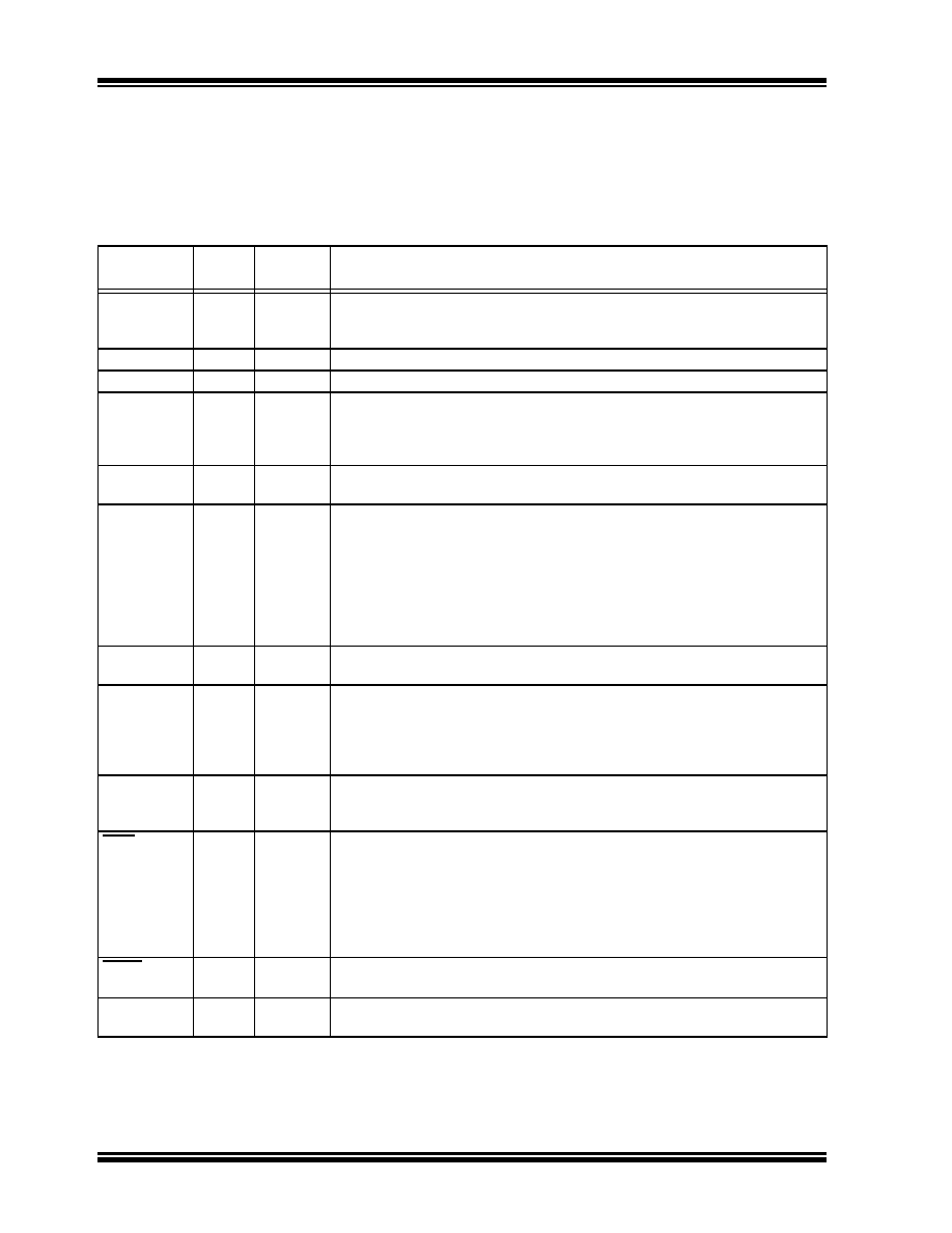
Table 1-1 provides a brief description of the device I/O
pinout and the functions that are multiplexed to a port
pin. Multiple functions may exist on one port pin. When
multiplexing occurs, the peripheral module’s functional
requirements may force an override of the data
direction of the port pin.
TABLE 1-1:
dsPIC30F3011 I/O PIN DESCRIPTIONS
Pin Name
Pin
Type
Buffer
Type
Description
AN0-AN8
I
Analog
Analog input channels.
AN0 and AN1 are also used for device programming data and clock inputs,
respectively.
AVDD
P
Positive supply for analog module. This pin must be connected at all times.
AVSS
P
Ground reference for analog module. This pin must be connected at all times.
CLKI
CLKO
I
O
ST/CMOS
—
External clock source input. Always associated with OSC1 pin function.
Oscillator crystal output. Connects to crystal or resonator in Crystal
Oscillator mode. Optionally functions as CLKO in RC and EC modes.
Always associated with OSC2 pin function.
CN0-CN7
CN17-CN18
I
ST
Input change notification inputs.
Can be software programmed for internal weak pull-ups on all inputs.
EMUD
EMUC
EMUD1
EMUC1
EMUD2
EMUC2
EMUD3
EMUC3
I/O
ST
ICD Primary Communication Channel data input/output pin.
ICD Primary Communication Channel clock input/output pin.
ICD Secondary Communication Channel data input/output pin.
ICD Secondary Communication Channel clock input/output pin.
ICD Tertiary Communication Channel data input/output pin.
ICD Tertiary Communication Channel clock input/output pin.
ICD Quaternary Communication Channel data input/output pin.
ICD Quaternary Communication Channel clock input/output pin.
IC1, IC2, IC7,
IC8
I
ST
Capture inputs 1, 2, 7 and 8.
INDX
QEA
QEB
I
ST
Quadrature Encoder Index Pulse input.
Quadrature Encoder Phase A input in QEI mode.
Auxiliary Timer External Clock/Gate input in Timer mode.
Quadrature Encoder Phase B input in QEI mode.
Auxiliary Timer External Clock/Gate input in Timer mode.
INT0
INT1
INT2
I
ST
External interrupt 0.
External interrupt 1.
External interrupt 2.
FLTA
PWM1L
PWM1H
PWM2L
PWM2H
PWM3L
PWM3H
I
O
ST
—
PWM Fault A input.
PWM 1 Low output.
PWM 1 High output.
PWM 2 Low output.
PWM 2 High output.
PWM 3 Low output.
PWM 3 High output.
MCLR
I/P
ST
Master Clear (Reset) input or programming voltage input. This pin is an active
low Reset to the device.
OCFA
OC1-OC4
I
O
ST
—
Compare Fault A input (for Compare channels 1, 2, 3 and 4).
Compare outputs 1 through 4.
Legend: CMOS =
CMOS compatible input or output
Analog =
Analog input
ST
=
Schmitt Trigger input with CMOS levels
O
=
Output
I
=
Input
P
=
Power
发布紧急采购,3分钟左右您将得到回复。
相关PDF资料
PIC18F4321T-I/ML
IC PIC MCU FLASH 4KX16 44QFN
PIC18F4221T-I/ML
IC PIC MCU FLASH 2KX16 44QFN
PIC18F2321T-I/ML
IC PIC MCU FLASH 4KX16 28QFN
PIC18F2221T-I/SO
IC PIC MCU FLASH 2KX16 28SOIC
PIC16LF1939-I/MV
IC MCU 8BIT 28KB FLASH 40-UQFN
PIC24F16KL402-I/SP
IC MCU 16BIT 16KB FLASH 28-SPDIP
PIC18F24J11-I/SS
IC PIC MCU FLASH 16K 2V 28-SSOP
PIC24F16KA101-I/SO
IC PIC MCU FLASH 16K 20-SOIC
相关代理商/技术参数
PIC18F4450T-I/PT
功能描述:8位微控制器 -MCU 16KB FL 768 RAM 34 I/O FS-USB 2.0 RoHS:否 制造商:Silicon Labs 核心:8051 处理器系列:C8051F39x 数据总线宽度:8 bit 最大时钟频率:50 MHz 程序存储器大小:16 KB 数据 RAM 大小:1 KB 片上 ADC:Yes 工作电源电压:1.8 V to 3.6 V 工作温度范围:- 40 C to + 105 C 封装 / 箱体:QFN-20 安装风格:SMD/SMT
PIC18F4455-BL
制造商:POWERLITE SYSTEMS 功能描述:PIC18F445 W/ BOOTLOADER FOR FLASHLAB 制造商:POWERLITE SYSTEMS 功能描述:PIC18F445 W/ BOOTLOADER, FOR FLASHLAB 制造商:POWERLITE SYSTEMS 功能描述:PIC18F445 W/ BOOTLOADER, FOR FLASHLAB; Silicon Manufacturer:Powerlite Systems; Core Architecture:PIC; Kit Contents:Board; Features:Bootloader Programming, RS232 Connector for Boot-Loading and Serial Comms ;RoHS Compliant: Yes
PIC18F4455-I/ML
功能描述:8位微控制器 -MCU 24kBF 2048RM FSUSB2 RoHS:否 制造商:Silicon Labs 核心:8051 处理器系列:C8051F39x 数据总线宽度:8 bit 最大时钟频率:50 MHz 程序存储器大小:16 KB 数据 RAM 大小:1 KB 片上 ADC:Yes 工作电源电压:1.8 V to 3.6 V 工作温度范围:- 40 C to + 105 C 封装 / 箱体:QFN-20 安装风格:SMD/SMT
PIC18F4455-I/P
功能描述:8位微控制器 -MCU 24kBF 2048RM FSUSB2 RoHS:否 制造商:Silicon Labs 核心:8051 处理器系列:C8051F39x 数据总线宽度:8 bit 最大时钟频率:50 MHz 程序存储器大小:16 KB 数据 RAM 大小:1 KB 片上 ADC:Yes 工作电源电压:1.8 V to 3.6 V 工作温度范围:- 40 C to + 105 C 封装 / 箱体:QFN-20 安装风格:SMD/SMT
PIC18F4455-I/PT
功能描述:8位微控制器 -MCU 24kBF 2048RM FSUSB2 RoHS:否 制造商:Silicon Labs 核心:8051 处理器系列:C8051F39x 数据总线宽度:8 bit 最大时钟频率:50 MHz 程序存储器大小:16 KB 数据 RAM 大小:1 KB 片上 ADC:Yes 工作电源电压:1.8 V to 3.6 V 工作温度范围:- 40 C to + 105 C 封装 / 箱体:QFN-20 安装风格:SMD/SMT
PIC18F4455T-I/ML
功能描述:8位微控制器 -MCU 24kBF 2048RM FSUSB2 RoHS:否 制造商:Silicon Labs 核心:8051 处理器系列:C8051F39x 数据总线宽度:8 bit 最大时钟频率:50 MHz 程序存储器大小:16 KB 数据 RAM 大小:1 KB 片上 ADC:Yes 工作电源电压:1.8 V to 3.6 V 工作温度范围:- 40 C to + 105 C 封装 / 箱体:QFN-20 安装风格:SMD/SMT
PIC18F4455T-I/PT
功能描述:8位微控制器 -MCU 24kBF 2048RM FSUSB2 RoHS:否 制造商:Silicon Labs 核心:8051 处理器系列:C8051F39x 数据总线宽度:8 bit 最大时钟频率:50 MHz 程序存储器大小:16 KB 数据 RAM 大小:1 KB 片上 ADC:Yes 工作电源电压:1.8 V to 3.6 V 工作温度范围:- 40 C to + 105 C 封装 / 箱体:QFN-20 安装风格:SMD/SMT
PIC18F4458-I/ML
功能描述:8位微控制器 -MCU 24KB Flash 2KB RAM RoHS:否 制造商:Silicon Labs 核心:8051 处理器系列:C8051F39x 数据总线宽度:8 bit 最大时钟频率:50 MHz 程序存储器大小:16 KB 数据 RAM 大小:1 KB 片上 ADC:Yes 工作电源电压:1.8 V to 3.6 V 工作温度范围:- 40 C to + 105 C 封装 / 箱体:QFN-20 安装风格:SMD/SMT